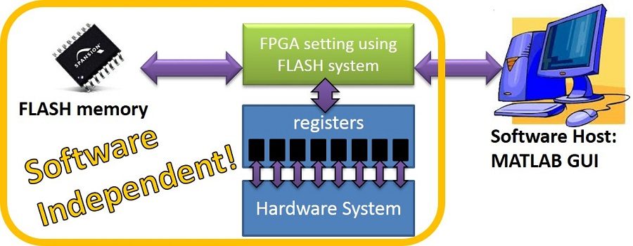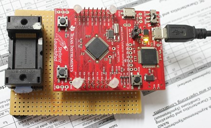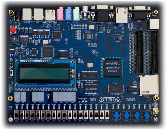
The FPGA setting using FLASH Project consists of 3 main parts: a software component (host), hardware on FPGA, and FLASH memory. The software component is a MATLAB based GUI for writing, reading, and erasing data on the FLASH memory. The hardware on the FPGA is the link between the software and the FLASH memory. It reads data stored in FLASH once power is turned on and configures on board clients....


