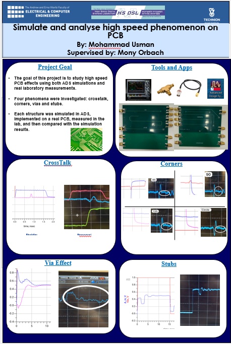
This project studies how high speed signals are affected by different PCB layout structures. Four phenomena were tested: crosstalk, corners, vias and stubs, using both ADS simulations and laboratory measurements. The comparison helps evaluate how accurately simulation predicts real PCB behavior.
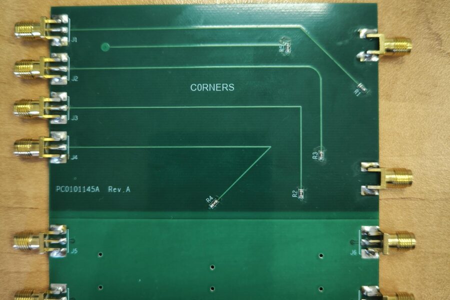
High speed PCB design requires understanding how the physical layout of the board affects signal integrity. In this project, four common PCB phenomena were investigated: crosstalk, corners, vias and stubs. Each one represents a different layout related effect that can change the signal waveform through coupling, reflections, delay or distortion.
The work started with ADS simulations. For each phenomenon, a dedicated layout was built, the substrate was defined, electromagnetic simulation was performed, and S parameters were extracted. The extracted models were then used in time domain simulations to observe the expected waveform behavior .
After the simulation stage, a real PCB was designed with structures similar to the simulated ones. The board was measured in the laboratory using a pulse signal, oscilloscope, cables and connectors. The measured results were compared with the simulated results in order to identify the main similarities and differences.
The results showed that ADS simulations can predict the main behavior of the tested PCB structures, while real measurements also include additional effects caused by the measurement setup. Overall, the project demonstrates the importance of combining simulation and practical testing when analyzing high speed PCB signal integrity.