Risc-V experiment project with a main goal of developing a lab experiment for the HSDS laboratory. The experiment’s purpose is to teach students and show them in detail how exactly the Risc-V processor works.

The project’s main goal is developing a lab experiment for the HSDS Laboratory.
The experiment’s purpose is to teach students and show them in detail how exactly the Risc-V processor works.
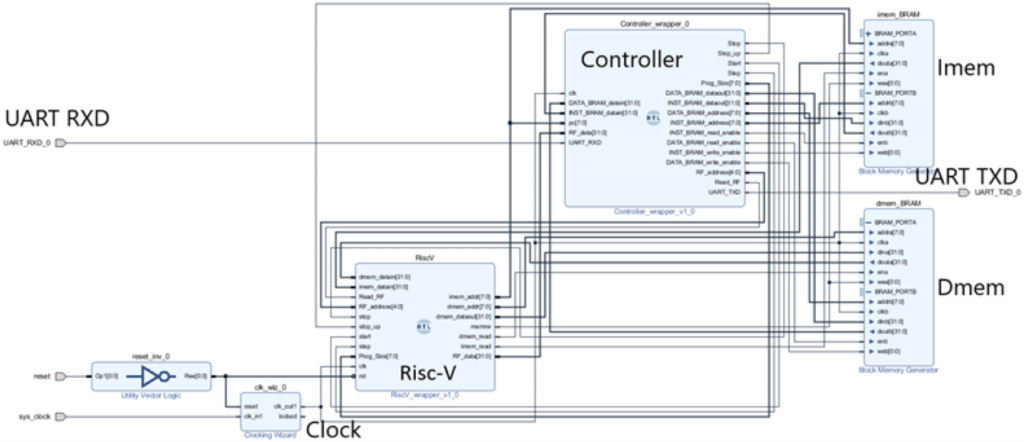
Vivado’s environment tools were used in order to write and debug HDL code, burn it on an FPGA and communicate with the computer.
Changes were needed for the Risc-V implementation from the course – Logic Design of Computer Structure to make it synthesizable so it could be burned on the FPGA.
It required an addition of two BRAMs – memory blocks modules that are implemented on the FPGA.
The communication between the computer and the FPGA is through the UART protocol, which was implemented in a controller module that controls all the data transfer between them. The data is being transferred through a TeraTerm terminal.
There are 2 types of supported commands, Risc-V control commands and Memory control commands. Among the Risc-v commands you could find for example- Start/Stop the processor, reading register values and more. Memory commands for example are- Instruction read/write and Data read/write.
This project created a convenient testing and debugging environment for students that allows them to deepen their knowledge and understanding of the functions that being supported by the Risc-V.


