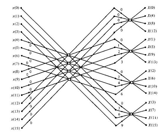
The project goals is to design and implement on FPGA device FFT that capable to deal with high rate data processing (rates up to 10MSamp/sec*). *- 5Ms/sec for each of I and Q components .

This implementation results in minimal number of multipliers (DSP slices). In the FFT core used real multipliers. Complex multipliers was generated in Xilinx IP core generator (LogiCORE IP Complex Multiplier v3.1), this complex multiplier utilize only 3 real multipliers instead of four multipliers needed to calculate complex multiplication.
The second parameter for choosing this architecture was the ability to achieve high operational rates. FFT core capable to operates onclock , this leads to the following data throughput capacity
All arithmetic calculation performed in 2’s complement fixed point data format. In order to prevent overflows during subtractions/additions data buses were expanded from stage to stage correspondingly. In current FFT implementation multiplication don’t results in data expansion width due to the fact that all multiplication performed with twiddle factor and it varying in [-1,1]. The multiplication result no greater that the largest of two multiplicands , therefore number of bits for the number representation stay the same.

