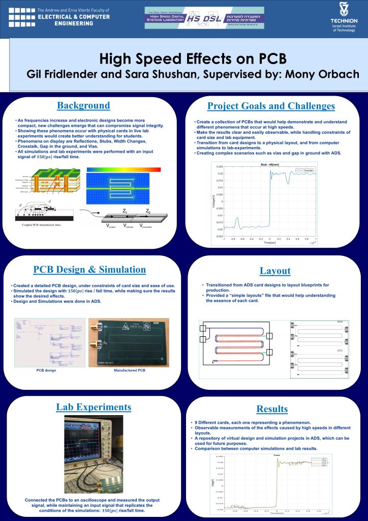
Demonstration of various high-speed phenomena in PCBs, through design, simulation, layout, and laboratory experimentation.
The project was done with the objective of demonstrating a variety of high-speed phenomena that occur within printed circuit boards (PCBs). It was done using a systematic approach of multiple stages for each phenomenon: design, simulation, layout, and laboratory experimentation. Through these stages, the project aimed to replicate real-world conditions and behaviors within PCBs, allowing future students to better understand the effects of high-speeds on PCBs.
The phenomena on display in the project are reflections, stubs, width changes, crosstalk, gap in the ground, and vias. Each phenomenon is represented in a dedicated PCB card, designed to make an observable change in measurement.
During the design and simulation stages, a detailed description of each circuit was created, taking into account real-world constraints such as card size and lab frequencies. Simulations were then performed under conditions that aimed to replicate those constraints, while aiming to achieve an easily observable measurement of the phenomena.
The layout stage further refined these designs, transitioning from theoretical concepts to tangible PCB layouts. Each card layout was created to demonstrate a phenomenon that was previously simulated, with the aim of presenting visible results in the lab experiments. This stage ensured a smooth transition from computer simulations to lab experiments.
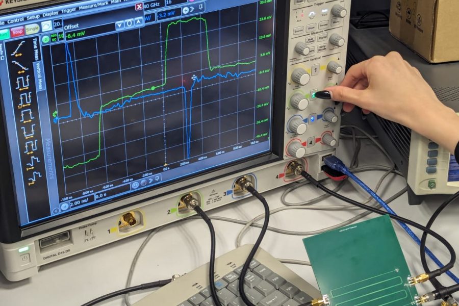
During the laboratory experiments stage, the PCBs were put to the test – the cards were connected to an oscilloscope under conditions that aimed to replicate the ones in the simulations. The measurements from the lab were analyzed and compared to the simulated outcomes, showing the alignment between the simulated predictions and the real-world results.
Ultimately, the project’s goal was to deepen the understanding of the effects high speeds have on PCBs for future students, by making the different phenomena observable and easily measurable. By following a strict methodology, each phenomenon was carefully processed, leading to a final product of user-friendly PCB cards, and a repository of virtual design and simulation projects.