The project goal is to sample with fast A/D to PC memory at highest possible speed.
This project presents the process of designing and implementing a fast A/D system, that samples into a binary file on a hard drive of a Host PC using the FMC125 board as the sampling device and the ML605 Virtex-6 evaluation board as the mediator between the FMC125 and the PC. The solution was implemented with a host SW commanding a firmware resident on a soft-core processor on the Virtex6 FPGA with high level commands. The firmware is in turn responsible for activating the systems hardware.
The project consists of two mostly separate parts:
- Sampling data in high speed data rate and storing it in ML605 on board DDR3 memory.
- Transferring the data from ML605 memory to PC memory via PCI-Express, and writing it to a binary file.
We divided the first item into several stages:
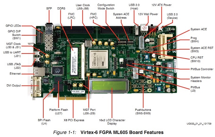
- Getting familiar with the development board, running BIST applications.
- Functionality demonstration of on board memory.
- Study of the FMC125 and its reference design.
- Functionality demonstration of the FMC125 within our system.
- Finally, writing the sampled data into memory.
The second item was mainly about taking the data stored in the on board memory and transfer it to the PC memory through PCIe. Another requirement was to provide communication with the Host PC through PCIe and write the Host software to control the system and output the received data to disk.
The stages we divided the second item into:
- Learning Xilinx PCIe solution.
- Provide the communication capability in the system.
- Study Jungo WinDriver, in particular setting up DMA.
- Transfer the data stored in on board memory to PCIe core and PC memory.
- Create a GUI with control and file output capabilities
The FPGA design was implemented using Xilinx ISE project navigator, Xilinx Platform Studio (XPS) for the embedded part of that system, Xilinx Software Development Kit (SDK) for the firmware. A summary of our experiences with the software is located in the conclusions section in our report.
We encountered many issues during this project; one of them was the lack of proper documentation of Xilinx products, and the steep learning curve for their tools. We had to be creative with our design solutions and overcome the lack of experience we both had.
Another problem was the project’s very high bandwidth requirements from the ADC to memory, which were bordering on impossibility. Xilinx IP’s were lacking the required performance capabilities for the project data bandwidth requirements, so we had to design our own high performance bus mastering DMA core that complies with the AXI4 standard.
Another difficulty was 4DSP choice to use a non-standard interface for their reference design for the FMC125 board. It forced us to create a translator core for enabling communication with the part taken from the reference design.