This project presents the design, analysis and testing of a PCIe 4.0 PBERT clock source module. The design includes two PLL synthesizer modules and a controller. The first module outputs a clean 200MHz clock for an FPGA, while the second outputs a 16GHz data-rate clock. The 16GHz clock can be output very clean (less than 10mUI) or modulated to add random or deterministic jitter as desired.
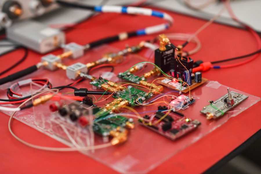
To test the reliability of a data-channel, one of the most useful pieces of equipment is a Bit Error Rate Tester (BERT). The concept is to send a random bitstream through the channel and compare what comes through the channel with what was sent. One can test additional properties of a channel’s transmitter and receiver by adding jitter to the input bitstream in what’s known as a jitter-BERT (jBERT). Finally, equipment can also be designed to send valid message packets through the channel and analyze how the error rate and jitter affect the protocol in what’s known as a Protocol-BERT (PBERT). A PBERT can be broken down into four major sections: 1) PC – for control and user-interface 2) FPGA – Control logic and data capture and analysis. 3) Clock source – with adjustable jitter. 4) Data alignment block – to add jitter to the bitstream. The clock source block can be further broken into five major sub-blocks being; a block controller, a 10MHz reference clock source, a noise source for random jitter (RJ) injection, and two synthesizer modules. The first synthesizer creates a clean 200MHz source for the FPGA to lock to, and the second module creates the 16GHz data-rate clock which can be clean (less than 10mUI RMS RJ), or with added jitter. The scope of this project is the two clock synthesizer modules and the associated controller. One of the major goals in the project was to use readily available parts and low-cost materials such as FR-4.


