Designing and implementing Dual Port FIFO on FPGA, designing a tester module
and comparing to a commercial Xilinx FIFO using the tester module.
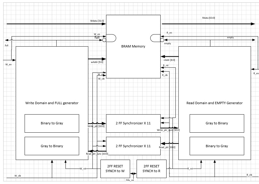
FIFO is a basic, common building block that exists mostly to synchronize data transfer from different time domains.
Synchronous FIFO reads data at the same clock as writing data, and
therefore the memory is easy for management.
A-synchronous FIFO works in 2 different clock frequencies. In order to
manage memory at any given time, it is crucial to keep track of the write and
read pointers to the memory and synchronize them to the other time
domain and compare them.
Using the comparison, it is possible to tell whether the memory is empty, full, or neither.
Without synchronizing pointers, the design is prone to metastability
problems, meaning hold/setup time aren’t always kept and FF output is unpredictable.
This can compromise the system’s logic functioning.
This project comprised of using SV to design an A-sync FIFO with write clock of
66[MHz] and read clock of 100[MHz]. In write clock the FIFO writes 32 bits, and in
read clock it reads 64 bits.
The data is then written into Xilinx Dual Port BRAM memory block with depth of 1024 words. Xilinx FIFO IP is used as reference for a functioning FIFO.
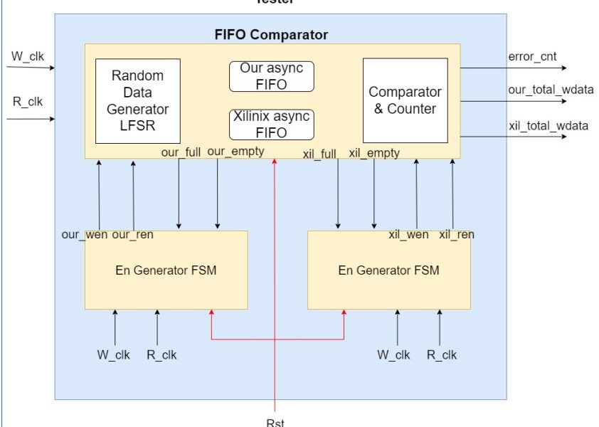
Designing a tester module allows us to create a testbench for FPGA in order to compare between the project’s FIFO and Xilinx’s.
After design and simulations, the FIFO is synthesized and implemented over FPGA and debugged using ChipScope until the same results
as Xilinx’s module are received.