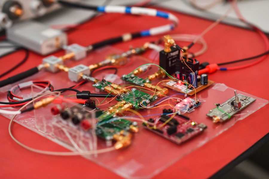
This project presents the design, analysis and testing of a PCIe 4.0 PBERT clock source module. The design includes two PLL synthesizer modules and a controller. The first module outputs a clean 200MHz clock for an FPGA, while the second outputs a 16GHz data-rate clock. The 16GHz clock can be output very clean (less than 10mUI) or modulated to add random or deterministic jitter as desired.