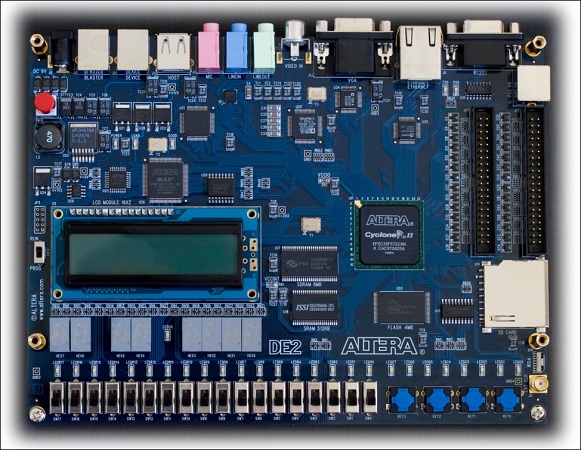
Designing a controller for flash memory that implements reading, writing and erasing.
The Flash memory technology is very common and popular these days. Its popularity keeps growing with the recent introduction of high capacity SSD drives that put it in direct competition with the familiar Hard Drives that can be found in almost every PC. A major disadvantage of the Flash technology in this competition is its inferior durability. In this project, this durability is put to the test using a controller specially designed to wear a Flash device by repeated write-erase cycles. In addition, a possible solution in the form of using Write Once Memory (WOM) codes is proposed. Since Flash durability is limited by the amount of times each cell can be erased, the use of WOM codes can prolong device life by reducing the amount of erases necessary between writes. The expected improvement in the endurance is then quantified and presented.