Scan Insertion is a powerful product testing technique commonly used nowadays. Unfortunately, when security is a concern, scan insertion may pose a major problem. In our project, we exploited this vulnerability for reverse engineering purposes.
Most of the digital VSLI devices nowadays uses a technique called ‘scan insertion’ for product testing purposes. The algorithm chains the internal registers of entire implementation into several shift registers called ‘scan chains’. Thus, we can build a tester which uses the scan chains for driving input and state to the combinatorial circuits, sampling and checking product output with the expected output. The technique allows testing chips for correct behavior and reaches high fault coverage which makes the scan insertion a very reliable testing method.
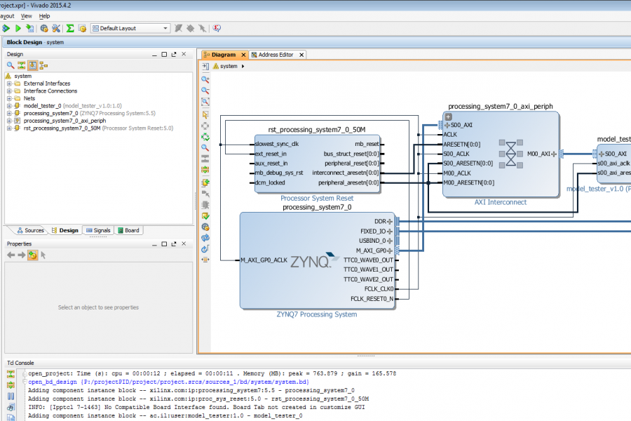
We exploited the security problems of the scan technique for reverse engineering purposes. We designed a tester on a FGPA platform, which performs scan tests of VLSI devices following the scan insertion protocol. The tester receives a scan input, drives it to the tested device and sends the scan output to a processing algorithm. The algorithm is implemented on the ARM processor of the board, it generates input vectors for the tester and learns the tested model truth tables and its implementation.
We demonstrated that by attacking the scan channel, we are able to extract the hardware internal registers behavior paving the way to reconstructing the VLSI product implementation and uncovering confidential information, cryptographic keys and commercial secrets.
