Nowadays, many VLSI (Very Large Scale Integration) components are manufactured in the industry. After manufacturing these components, there is need for component validation before composition in a larger system, or delivering the products to the client.
In spring 2009, VLSI Lab offered a Tester for VLSI components project to HSDSL. In our project, the main idea was to create a custom HW and SW solution that will allow examining different components. The tester project includes an ASIC* daughter board (HW) that is connected to an FPGA in the HSDS lab, and the different DUTs (device under test) will be connected to this board. The interaction with the components will be from an application (SW) to the FPGA, from the FPGA to the daughter board (written in VHDL) and from the DB to the DUTs through the board's pins that are connected to the components.
The project was divided to two parts and was given to two groups that together formed the project's entire group:
• Hardware group – in charge of developing the daughter board and creating the interaction with the FPGA (VHDL).
• Software group – in charge of developing the host application, which will enable the end user to test his component.
Eventually, these two parts are combined to one end-to-end project.
This document concludes the development of the SW part of the tester project.
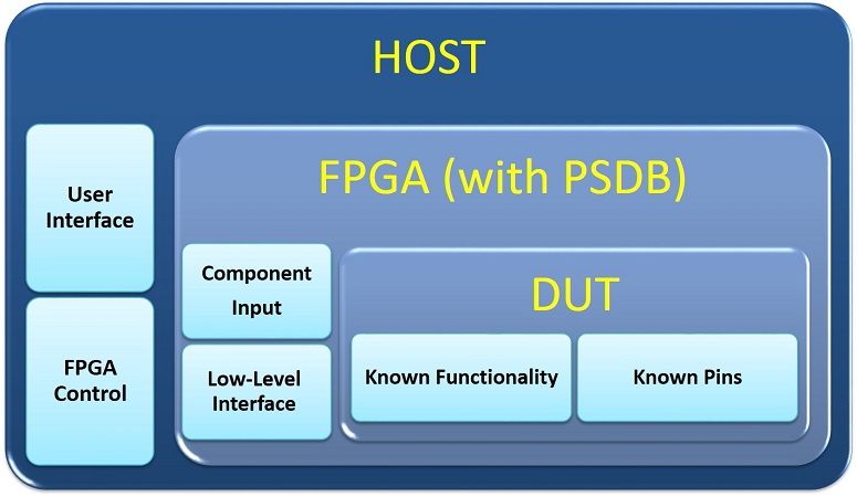
The main goal of the project is to develop an end-to-end tester that will allow testing the functional correctness of different components.
Under the main goal, our project goal was to develop the entire SW part:
- Design the host application for the tester.
- Define the interface and protocol, with the HW group, for interaction with the HW.
- Develop a GUI which will allow to:
- Define the pins configuration – inputs and outputs (connected to the board)
- Determine the test vectors.
- View output vectors
- Compare the outputs to wanted outputs (functional correctness).